
Highly Efficient On-Chip Electronic-Plasmonic Transducers
Opportunity
In recent years, emerging technologies such as artificial intelligence (AI) and Internet of Things (IoT) have exerted increasing demands on semiconductor technology-for greater processing power and smaller chips. Growing consumer purchasing power for compact and powerful electronics have likewise contributed to this trend. The global market for semiconductors was estimated to be US$425.96 billion in 2020, and growing at a CAGR of 8.6% to reach US$803.15 billion by 2028.
However, with silicon electronics reaching their fundamental limits, alternatives are needed for the semiconductor industry to keep up with current needs and demands. One such option is plasmonics, which offers high speeds at compact sizes for integrated circuits. Yet, existing approaches are slow and inefficient-rendering them impractical for use.
Technology
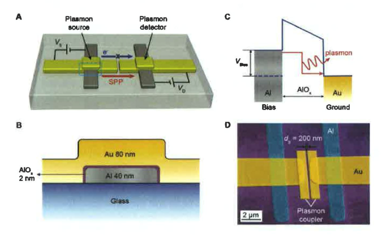
This invention consists of on-chip electronic-plasmonic transducers based on quantum mechanical tunnel junctions. The metal-insulator-metal (MIM) tunnel junctions are directly coupled to plasmonic waveguides, which enable efficient on-chip generation, manipulation, and read-out of plasmons.
With plasmon-assisted tunnelling, the transducers demonstrate plasmon generation and read-out efficiencies of 10% to 20%. As they work on quantum mechanical tunnelling time scales, the transducers are one thousand times faster than conventional semiconductor devices, have low power consumption and are compact.
Furthermore, by integrating two of the MIM junctions along a plasmonic coupler, an integrated plasmon-based frequency doubler transducer can be formed. The integrated doubler transducer devices show an overall efficiency of 4.9% to 6.5%-close to that of transistor-based frequency multipliers.
On-chip plasmonic-electronic transducer

Download
