

Techniques to Modulate Spin Orbit Spin Transfer Torques for Magnetization Manipulation
Opportunity
In modern spintronic devices, such as information storage devices (e.g. random access memory), the magnetization directions of ferromagnets (FMs) are utilized to write, store and retrieve information. Effective manipulation of the magnetization direction, e.g. switching the magnetization direction via interaction between spin and charge, is important to the operation of such devices. Traditionally, magnetization manipulation has been achieved via current induced spin transfer torque (STT) that requires a ferromagnetic spin polarizer in a spin valve or magnetic tunnel junction structure. Recently, techniques have been developed for magnetization manipulation that utilize spin orbit spin transfer torque (SO-STT). A typical SO-STT spintronic device is structured as a multilayer stack including a ferromagnet (FM) layer adjacent to a metal layer (also referred to as an under or capping layer), among other layers. When a charge current flows through the SO-STT device, a spin current from the adjacent metal layer diffuses into the FM layer and influences the magnetization of the FM. The use of such an arrangement provides various advantages, for example, allowing for low power magnetization manipulation and fast motion of domain walls. In addition, the SO-STT technique allows for separate writing and reading current paths.
While SO-STT is a powerful technique for electrically manipulating magnetization in spintronic devices, there is a need for improved ways of modulating SO-STT. Traditionally, SO-STT devices have required an external magnetic field, referred to as a "symmetry breaking" external magnetic field, to be applied to the device to be able to switch magnetization in a deterministic way. If this requirement can be eliminated, it will allow for greater simplification of the device's multilayer stack, which can simplify the fabrication process and/or improve device reliability. Likewise, traditional SO-STT devices require higher than desired SO-STT switching current density. Improved techniques to enhance and modulate SO-STT magnitude are highly desired for low power spintronic devices (e.g., ultra low power magnetoresistive random-access memory (MRAM) devices) and/or high density magnetic storage devices.
Technology
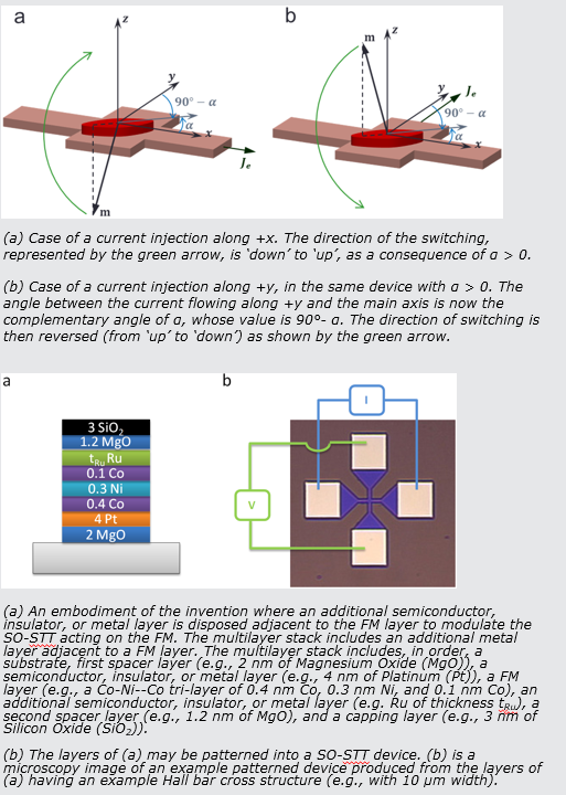
The need for a "symmetry breaking" external magnetic field may be avoided in a SO-STT device by implementing a non-symmetric device geometry. The non-symmetric device geometry may be produced by tilting a shaped magnetic pattern (e.g., an ellipse, diamond, rectangle, etc. shaped magnetic pattern) such that the pattern's main (long and short) axes are tilted with respected to an in-plane current direction, which may create triaxial anisotropy. The second anisotropy (additional to traditional perpendicular magnetic anisotropy) may replace the external magnetic field to provide deterministic SO-STT switching. Alternatively, the non-symmetric device geometry may be produced by locating the magnetic pattern away from the center of a current injection line. A SO-STT device (e.g., a 4-terminal device), made of the two current injection lines disposed at a non-zero angle with respect to each other (e.g., orthogonal current injection lines) and an ellipse-shaped magnetic pattern showing perpendicular magnetic anisotropy, located in the central part of the cross, allows for writing "up" or "down" magnetization states with current pulses with no requirement for an external assist field. as well as reading through anomalous Hall resistance or magnetic tunnel junction structures on top of the FM layer.
The SO-STT device that uses a non-symmetric (e.g. tilted ellipse) device geometry may be further improved by integrating an additional semiconductor, insulator or metal layer into the device's multilayer stack for giant modulation of SO-STT. By integrating the additional semiconductor, insulator or metal layer, a significant reduction of SO-STT switching current density may be achieved. Depending on the embodiment, the additional semiconductor, insulator or metal layer may be disposed adjacent to the FM layer, or within the FM layer, among other possibilities.

Download
