

Controlled and Selective Etching of Crystalline Silicon at Nanoscale
Opportunity
Increasing demand for smartphones and smart consumer electronics such as wearables, tablets and handheld devices underpins the strong growth of the global semiconductor market—in spite of the COVID-19 pandemic. Expanding at a CAGR of 4.5%, the global semiconductor market size is projected to reach US$726.73 billion by 2027.
However, for this potential to be realised and Moore’s Law to continue on its trajectory, more precise processes are needed for etching semiconductors. Presently, conventional etching is done through dry etching by plasma. While this allows for circular structures, the process also damages the surface. In smaller structures, this surface damage becomes unacceptable. This is because with the drastic increase in surface-to-volume damage ratio, it will mean that most of the channel is damaged.
Wet etching presents an alternative to dry etching as it can produce nanostructures without surface damages. However, existing methods exhibit non-isotropic etching behaviour, in which planes are etched at different speeds. This results in unwanted facets or anisotropic thinning of the nanopillars/nanowires formed. So far, attempts to overcome these issues have shown limited success.
Technology
This novel technology proposes a method for etching single crystalline silicon (c-Si) in potassium hydroxide (KOH) solution. To prevent unwanted faceting of the nanopillars, the crystalline silicon in the etchant solution is stirred in an oscillatory manner alternated with periods without stirring.
It is demonstrated that agitation of the etchant during wet-etching (e.g. by stirring it) plays a critical role in controlling the anisotropy of c-Si nanopillars etched in KOH solution. Stirred and non-stirred results show a 45° rotation in the etch anisotropy of c-Si—a complete switching of the etch direction from the (110) and (100) crystallographic planes of silicon. By utilising this controlled switching in etching direction, it is possible to maintain the circularity of the nanopillars while thinning them down to sub-10 nm diameters. Switching to another etchant for etching silicon in a different crystallographic direction is not required.
This method is suitable for future microelectronic devices with gate-all-around (GAA) and 3D silicon architectures. Furthermore, it solves the longstanding problem in microelectronic manufacturing of needing controlled and selective etching—which has only gotten more urgent with ongoing changes in the design of microelectronics.
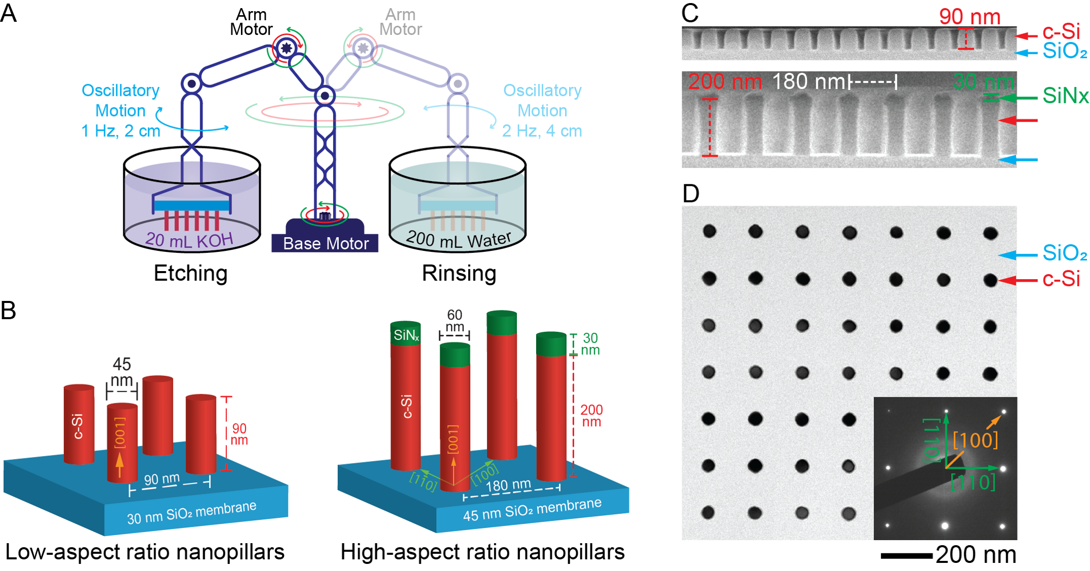
Illustration of equipment setup, samples used, SEM and TEM images of the resulting Si nanopillars produced

Download
